FPGAs 2: Multiplexed RGB LED Panels
Sat, Apr 4, 2020 Companion code for this post available on GithubOne of the more eyecatching demonstrations of FPGAs recently has been the trend to show off smoothly animating LED Cubes of various sizes and shapes. But what goes into making these? How do we interface with the LED panels that construct them? And can we use those panels to show an animated GIF? In this post, I will attempt to cover the building blocks necessary to load custom animations onto a FPGA board powered by the Lattice HX4K, and display those animations on a 64x64 LED panel. All source code for the following can be found on Github.
How do RGB panels work?
While the specific layout of the various LED panels available online may differ, the general architecture is by and large the same. Three sets of shift registers (one each for the red, green and blue pixel data) have each bit of their output connected across one column of the LED grid. This means that whatever bit pattern is shifted into these registers controls which columns of the display will light up. However, we generally don’t want to the same data on every line - in order to select a single row for the given column data, the common pin of each LED in a row is connected to an output of an address demultiplexer, which uses the address select inputs to enable only a single row at a time. A simplified diagram of a 64-column by 32-row display is shown below (many rows/cols have been omitted):
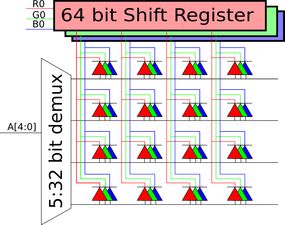
Subsection of common RGB panel
One thing to note about this architecture is that while it is simple in terms of component cost, we can only actually display one unique row of data at a time. In order to show an entire image, we need to quickly scan through displaying rows at some speed above which the strobing is invisible to the naked eye, and the persistence of vision effect makes the image appear solid. This sort of high speed data shifting application is a perfect place for FPGAs, so in the rest of this post we will try and cover getting from displaying a solid colour to full animated GIFs with 5 bit colour channels.
If you want to follow along, I would strongly suggest building one of the ICE40 HX4K Breakout Boards I wrote about here, which the code samples in this post have been written for, or a comparable board such as 1bitsquared’s iCEBreaker.
You will also need a LED panel - the one I will be using here is a 64x64 model with a HUB75E connector. You can find similar panels cheaply on AliExpress (search HUB75E, 64x64), or purchase find them at various other sellers on the internet. This panel is internally organized as two 64x32 panels, so instead of having just the one set of RGB shift registers it instead has two, one for the top half and one for the bottom. This doesn’t mean too much for our design, we will just have two sets of outputs.
Finally, you will need some way to connect your FPGA board to the display. You can either use jumper wires or a PMOD style breakout, such as this one.
Getting started
The first thing to do with any project is get to the point where you can see everything working (or not working) end to end. So let’s start by creating a panel driver module that will cycle through displaying each of the 8 primary colours (the possible permutations of R, G, B) in turn to make sure that we are able to shift data in and advance the row selector. The first step in this is to configure which pins on our FPGA board connect to what signals of our LED panel. For me, I have the PMOD to HUB75E board connected to PMOD ports C1 and C2 on the HX4k Breakout board, as shown:
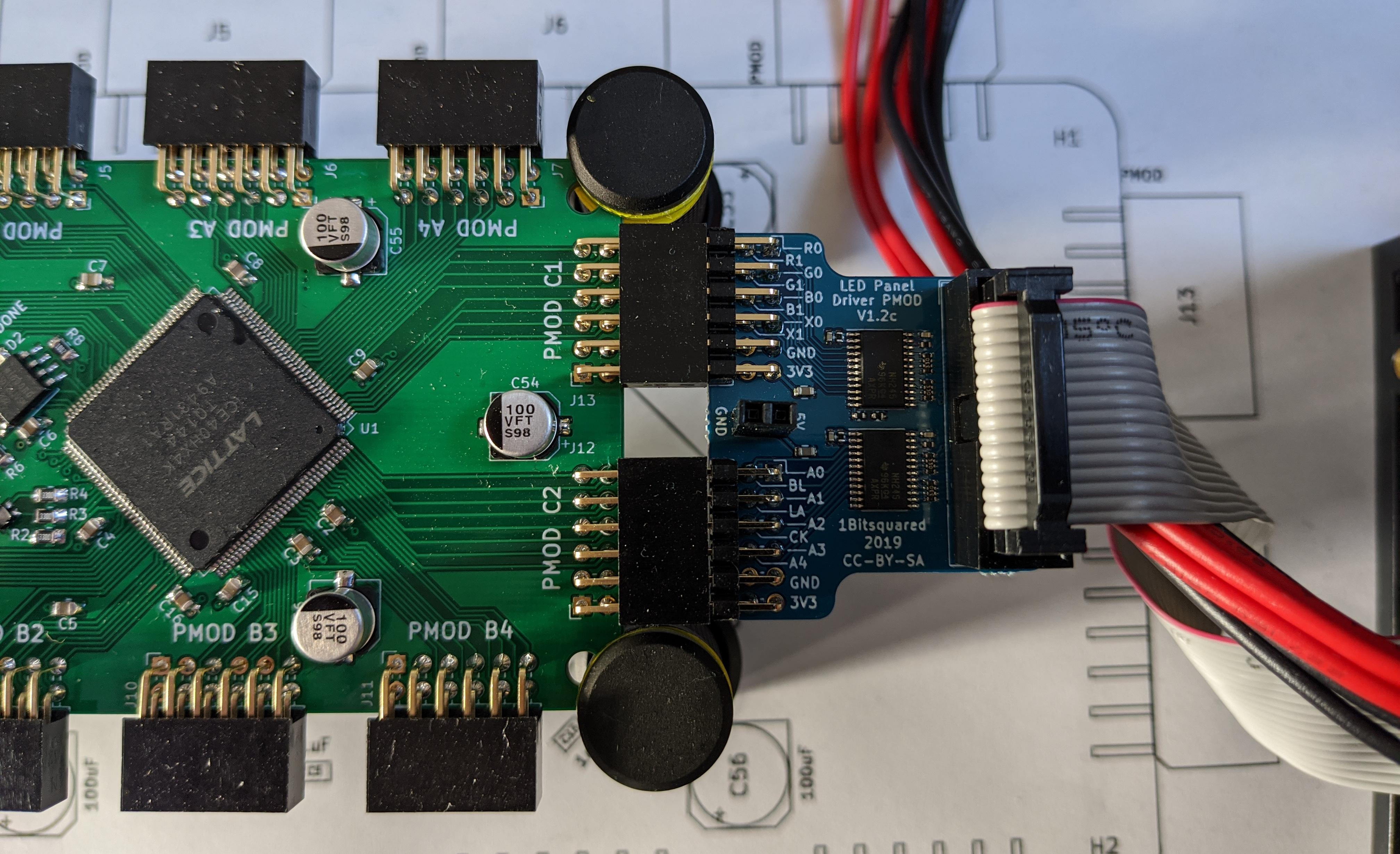
PMOD to HUB75E adapter
This means that I can use the PMOD[] definitions from the
Placement Constraint File
for the board when interfacing with the RGB panel. So in my top level verilog
file, I can declare my inputs like so:
module top(
        // Input clock
        input wire CLK_12MHZ,

        // PMODs
        output wire [7:0] PMOD_C1,
        output wire [7:0] PMOD_C2
    );

    // Map those PMOD pins to some real signal names
    wire [1:0] rgb_panel_r = {PMOD_C1[4], PMOD_C1[0]};
    wire [1:0] rgb_panel_g = {PMOD_C1[5], PMOD_C1[1]};
    wire [1:0] rgb_panel_b = {PMOD_C1[6], PMOD_C1[2]};
    wire [4:0] rgb_panel_a = {PMOD_C2[7],
                              PMOD_C2[3],
                              PMOD_C2[2],
                              PMOD_C2[1],
                              PMOD_C2[0]};
    wire rgb_panel_bl = PMOD_C2[4];
    wire rgb_panel_la = PMOD_C2[5];
    wire rgb_panel_ck = PMOD_C2[6];
With our IO named in the top module, let’s create a second module to hold all
of the logic needed to drive out display, called panel_driver. To start, we
will just try and display solid colours, one after the other. Here is the full
verilog description of that module:
`default_nettype none
`define CLOCK_HZ 12_000_000
module single_colour_test(
    // Input clock to our panel driver
    input wire i_clk,
    // Shift register controls for the column data
    output reg o_data_clock,
    output reg o_data_latch,
    output reg o_data_blank,
    // Data lines to be shifted
    output reg [1:0] o_data_r,
    output reg [1:0] o_data_g,
    output reg [1:0] o_data_b,
    // Inputs to the row select demux
    output reg [4:0] o_row_select
);

    // How many pixels to shift per row
    localparam pixels_per_row = 64;

    // State machine IDs
    localparam
        s_data_shift = 0,
        s_blank_set = 1,
        s_latch_set = 2,
        s_increment_row = 3,
        s_latch_clear = 4,
        s_blank_clear = 5;

    // Simple colour cycling logic. We will have a prescaler that counts down
    // to zero twice per second, based on the frequency of our module input
    // clock (`CLOCK_HZ`).
    // Whenever this countdown hits zero, we will increment our colour state
    // register, each bit of which is mapped to the reg, green or blue data
    // channel of the RGB panel shift registers.
    localparam COLOUR_CYCLE_PRESCALER = (`CLOCK_HZ / 2) - 1;
    reg [$clog2(COLOUR_CYCLE_PRESCALER):0] colour_cycle_counter = 0;
    reg [2:0] colour_register;
    always @(posedge i_clk) begin
        if (colour_cycle_counter == 0) begin
            colour_register <= colour_register + 1;
            colour_cycle_counter <= COLOUR_CYCLE_PRESCALER;
        end else
            colour_cycle_counter <= colour_cycle_counter - 1;
    end

    // Connect the output colour data lines to our colour counter
    assign o_data_r = {colour_register[0], colour_register[0]};
    assign o_data_g = {colour_register[1], colour_register[1]};
    assign o_data_b = {colour_register[2], colour_register[2]};

    // Register to keep track of where we are in our panel update state machine
    reg [2:0] state = s_data_shift;
    // How many pixels remain to be shifted in the 'data_shift' state
    reg [7:0] pixels_to_shift = 64;
    always @(posedge i_clk) begin
        case (state)
        s_data_shift: begin // Shift out new column data for this row
            if (pixels_to_shift > 0) begin
                // We have data to shift still
                if (o_data_clock == 0) begin
                    // For this test, we have hardcoded our colour output, so
                    // there is nothing to do per-pixel here
                    o_data_clock <= 1;
                end else begin
                    o_data_clock <= 0;
                    pixels_to_shift <= pixels_to_shift - 1;
                end
            end else
               state <= s_blank_set;
         end
         // In order to update the column data, these shift registers actually
         // seem to require the output is disabled before they will latch new
         // data. So to perform an update, we have a series of steps here that
         // - Blank the output
         // - Latch the new data
         // - Increment to the new row address
         // - Reset the latch state
         // - Unblank the display.
         // Each step has been made it's own state for clarity; if one wanted
         // to save a little more on logic some of these steps can be merged.
         s_blank_set: begin o_data_blank <= 1; state <= s_latch_set; end
         s_latch_set: begin o_data_latch <= 1; state <= s_increment_row; end
         s_increment_row: begin o_row_select <= o_row_select + 1;
                                state <= s_latch_clear; end
         s_latch_clear: begin o_data_latch <= 0; state <= s_blank_clear; end
         s_blank_clear: begin
             o_data_blank <= 0;
             pixels_to_shift <= pixels_per_row;
             state <= s_data_shift;
         end
        endcase
    end
endmodule
If we build and deploy this to our FPGA test board, we should see the connected LED panel flash through the 8 possible colours we have with each color channel being fully on / off:
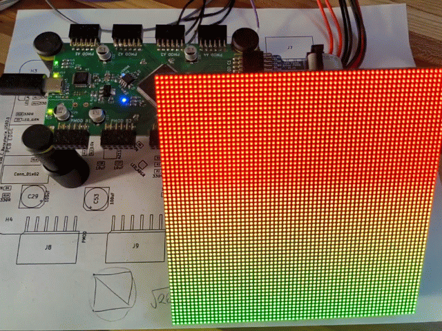
Full-colour test pattern
Displaying Images
So far so good - we are now able to control the colours output to the panel, and can do so fast enough that the panel appears to be solid. However, so far we are just displaying solid colours - not very useful. Instead, let’s add the ability for our gateware to display one of the most popular image formats: the animated GIF.

Our test image: nyancat
But this begs the question, how do we get all that data loaded into our FPGA? And once it’s in there, how do we display it? If we were to store each frame of the above GIF as a 64x64 array of bytes, we would need 64 * 63 * 3 * 11 frames of data - that’s 132 KiB. Looking at the datasheet for our HX4K, we see that it only has 80K ram bits - only 10K ram bytes! We will clearly need to be more creative. If instead of using a full byte per colour pixel we shave each channel down to 5, we can store one pixel in two bytes, using 5 bits each for Red/Green/Blue -> 15 bits per pixel. This brings us down to 88KiB for the entire animation, still far too large. However, it does bring us down to 8KiB per frame - which does fit in our 10KiB of system memory. But that still only fits one frame - in order to display an animation, we will have to have some persistent storage that we can read each frame from into our memory buffer so that we can blast it to the screen. Luckily, on this board, we have such a persistent storage - the flash chip used for storing the FPGA bitstream.
The HX4K bitstream is, at maximum, 136,448 bytes (according to Lattice note
TN1248)
. However, the flash chip on the HX4K breakout we are using here is 128 megabits,
or 16 megabytes. This means that even with the bitstream using the lower part
of the flash, we can store image data in the higher address regions so that our
application can read out frame data when it needs it. So let’s write a quick
program that, given a series of input images that are 64x64 pixels, converts
each one to a packed RGB565 and then writes all of the frames, in order, to a
binary file that we can then load onto the flash of the FPGA board. The full
source of this utility, img_pack, is included in the
Github repo
that accompanies this post. In order to use it on our test image, we first need
to do a little preprocessing using ImageMagick.
# Resize the gif to 64x64 pixels, ignoring aspect ratio
convert -resize 64x64\! nyan_fullres.gif nyan_64.gif
# Convert the resized gif into individual frames
# This will generate nyan_frame-0.png through nyan_frame-11.png
convert -coalesce nyan_64.gif nyan_frame.png
# Now that we have our individual frames as images, we can use the img_pack
# tool to generate a binary representation of the gif to be loaded to our board
img_pack nyancat.bin nyan_frame-{0..11}.png
After that, if you are using the HX4K dev board you can use the
faff
tool to load the program into flash at a safe offset that won’t interfere with
the FPGA bitstream itself.
If you are using the iCEBreaker board, the iceprog has a similar option for
loading data at a specific offset.
# To load the data into flash, we can use the faff utility to interact with the
# HX4K dev board, and write the data at offset 0x800000, safely out of the way
# of the bitstream
faff --lma 0x800000 -f nyancat.bin --no-verify
# Alternately, on an iCEBreaker, the following should work:
iceprog -o 0x800000 -X nyancat.bin
Reading from Flash
Now that the data is safely on the flash, we need to be able to actually access it from our FPGA, and then store it in our RAM buffer so that our panel driver can then read it and blit it to our display. The flash chip on the HX4K board, as well as those on almost all other flash chips, share a common set of command words. All of them can be found in the datasheet (see here), but the important ones here are:
0x66,0x99: Reset enable / reset. This command series will put the device back into a sane state to receive commands, important to do at boot since we can’t gauarantee what operation the flash was in the middle of whenever our gateware came online.0xAB: Release from power down. The HX4K, after loading the bitstream, is careful to put the flash chip into a power down state, since as far as it’s concerned it’s done with the flash until it next needs to load the bitstream. In order to read our frame data from it, we need to send this instruction to first wake it up.0x0B: Fast read. To get our pixel data out, we send this command followed by the 24 bit start address for our read, and then after one byte worth of delay the flash chip will output it’s data, one byte at a time, until we stop reading. When we need to read the next frame, we just send another fast read command and a new address, and we are good to go.
With these commands, we can think of our flash loader state machine as being:
- Idle state. Wait here until we get a signal to load the next frame from flash.
- Reset state. Select the flash chip, clock out the reset command.
- Wakeup state. Select the flash chip, and release it from power down.
- Initiate read state. Select the flash chip, and clock out the fast read command followed by the address data and the idle byte.
- Perform read. For as many bytes as are in a frame, shift in data and store it in our ram buffer. When we are done, return to the idle state.
A shortened version of the flash loader verilog is shown below. The full code listing can be found here.
// Flash commands for use later
`define FLASH_OP_RESET    16'H6699
`define FLASH_OP_FAST_READ 8'H0B
`define FLASH_OP_WAKEUP    8'HAB

always @(posedge i_clk) begin
    case (state)
        // Default idle state. This state will only transition if the 'initiate
        // read' module input is set, at which point it will latch the base
        // address and start the read operation
        s_idle: begin
            if (i_read_stb) begin
                flash_read_addr <= i_read_addr;
                state <= s_initiate_reset;
            end
        end

        // Perform a flash chip reset. Takes advantage of our
        // flush_command_buffer state, by just specifying the data to shift,
        // and which state to transition to after the command operation is
        // complete.
        s_initiate_reset: begin
            // Our command buffer just needs the two reset bytes, the rest
            // of the bits are don't care (zero)
            command_buffer <= {`FLASH_OP_RESET, 24'b0};
            cmd_buffer_bits_to_shift <= 16;
            flash_cs <= 0;
            // Once the command is done, we want to move to the wakeup step
            next_state <= s_initiate_wakeup;
            // Directly transition to the generalized 'flush buffer' state.
            state <= s_flush_command_buffer;
        end

        // Similar to the above, but takes the flash chip out of sleep mode
        s_initiate_wakeup: begin
            command_buffer <= {`FLASH_OP_WAKEUP, 32'b0};
            // [...]
            state <= s_flush_command_buffer;
        end

        // Once again, we set up the data for flush_command_buffer, this time
        // with the 'fast read' command and the start address we latched when
        // we started the read process
        s_initiate_read: begin
            command_buffer <= {`FLASH_OP_FAST_READ, flash_read_addr, 8'b0};
            // [...]
            state <= s_flush_command_buffer;
        end

        // State for performing a command action. Shifts out a given number of
        // bits from the command buffer (MSB first), and when done transitions
        // to the state idenfitied by the next_state register.
        s_flush_command_buffer: begin
            if (cmd_buffer_bits_to_shift > 0) begin
                if (flash_sck == 0) begin
                    // Latch new data and perform rising edge
                    {flash_mosi, command_buffer} <= {command_buffer, 1'b0};
                    flash_sck <= 1;
                end else begin
                    // Perform falling edge and decrement bit count
                    flash_sck <= 0;
                    cmd_buffer_bits_to_shift <= cmd_buffer_bits_to_shift - 1;
                end
            end else begin
                // Done - move to continuation state
                state <= next_state;
                // If we aren't moving to the read state, deassert CS
                if (next_state != s_shift_data)
                    flash_cs <= 1;
            end
        end

        // Here is where we actually handle the incoming data from the flash
        // chip. Each 16 bit word is one pixel, so every time we successfully
        // read 16 bits we write it out to a block memory using the
        // ram_address, ram_data and ram_write_enable signals.
        s_shift_data: begin
            // We are going to care about 16 bit chunks, since that's
            // the interface we're using for our block RAMs
            if (words_to_read == 0) begin
                ram_write_enable <= 0;
                flash_cs <= 1;
                state <= s_idle;
            end else begin
                if (input_bits_to_shift == 0) begin
                    // Done shifting a word, move it to the output data
                    // lines and strobe the write signal
                    ram_data <= input_shift_data;
                    ram_write_enable <= 1;
                    words_to_read <= words_to_read - 1;
                    input_bits_to_shift <= 16;
                end else begin
                    // If we just did a write, bring the strobe back down
                    // and increment the write address for next time
                    if (ram_write_enable) begin
                        ram_write_enable <= 0;
                        ram_address <= ram_address + 1;
                    end
                    if (o_flash_sck == 0) begin
                        // Set up rising edge of SPI clock
                        flash_mosi <= 1'b0;
                        flash_sck <= 1;
                    end else begin
                        // Falling edge
                        flash_sck <= 0;
                        input_shift_data <= {input_shift_data[14:0], i_flash_miso};
                        input_bits_to_shift <= input_bits_to_shift - 1;
                    end
                end
            end
        end
    endcase
end
Simulating our Flash reader
Since reading from a flash chip is slightly more involved than shifting out our pixel data, and a little harder to visually debug, let’s write a quick test interface in Verilator so that we can observe that our flash interface sends the right data with the right timings to initialize a flash read, and that it then takes the incoming data and stores it in the right place. Full source code for the testbench can be found here.
To make our I/O more realistic, in our testbench we can create a fake SPI chip that responds to read requests by keeping track of the output signals from the flash_loader verilog module. An annotated excerpt of the flash simulator is shown below:
// Data to to 'read'
const uint8_t *data =
    reinterpret_cast<const uint8_t *>("This is a test string");
const unsigned data_len = strlen(data);

// Fake flash update method, should be called after each master clock cycle of
// the simulation
void DummyFlash::eval() {
  // Did the CS state change?
  if (*spi_cs != last_cs) {
    fprintf(stderr, "CS state: was %u, now %u\n", last_cs, *spi_cs);
    // If the cs line went low on this clock cycle, then the flash chip is now
    // selected. Use this as a trigger to reset our fake flash state.
    if (*spi_cs == 0) {
      shift_byte_index = 0;
      shift_bit_index = 0;
      *spi_miso = 1;
      last_sck = *spi_sck;
    } else {
      // Deselected. Move the miso line to a known state.
      *spi_miso = 1;
    }
    // Keep track of changes to the chip select pin.
    last_cs = *spi_cs;
  }

  // If we aren't selected, just return
  if (last_cs == 1) {
    return;
  }

  // Did the clock transition?
  if (*spi_sck != last_sck) {
    last_sck = *spi_sck;
    if (last_sck) {
      // Posedge, increment the number of bits we have received from the
      // SPI master
      preamble_bit_count++;
    } else {
      // Negedge
      // Don't shift data if this is the read preamble
      if (preamble_bit_count >= 40) {
        // Set miso to be the next bit
        *spi_miso =
            data[shift_byte_index % data_len] &
              (0b1000'0000 >> shift_bit_index) ? 1 : 0;
        // Increment the bit index
        shift_bit_index++;
        // If we hit the end of the byte, increment the byte index
        if (shift_bit_index > 7) {
          shift_bit_index = 0;
          shift_byte_index++;
          fprintf(stderr, "New byte: %02x\n", data[shift_byte_index]);
        }
      }
    }
  }
}
In this simple flash example, we don’t actually verify the input address / reset state of the flash, but hopefully this example gives an idea of how the test code might be extended to perform this checking. If we then compile and run the full testbench with tracing enabled, like so:
# Build the CMake project that contains the Verilator testbenches
mkdir tb/build
cd tb/build
cmake ../
make -j$(nproc)
# Run the flash loader testbench. This will generate the flash_loader.vcd file,
# which can be examined in GTKwave
./tb_flash_loader
We get an output file that can be loaded into GTKWave, where we can observe the communication between our flash loader verilog, our emulated flash and the output signals to our pixel buffer memory. By looking carefully at these signals, we can be confident that our design will work once deployed on our actual FPGA board.
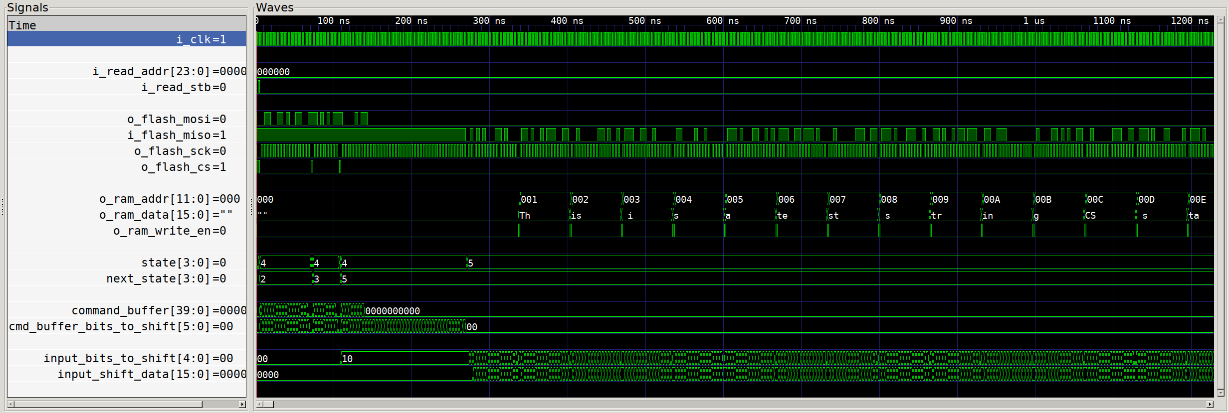
Trace of simulated flash loader reading from 'Flash'
Rendering from memory
With a module for reading our pixel data from flash, the only things remaining to get animated images running on our LED panel is an animating counter for triggering the load of the next frame, and then a modification to the panel driver code to use the loaded frame data.
// Animation counter for triggering frame loads from the flash chip
localparam ANIMATION_UPDATE_PRESCALER = (`clk_hz / 10) - 1; // 10fps
localparam ANIMATION_FRAME_COUNT = 11; // Number of frames in the animation
reg [$clog2(ANIMATION_UPDATE_PRESCALER):0] prescaler_reg = 0;
always @(posedge i_clk) begin
    if (prescaler_reg == 0) begin
        // Reload the prescaler downcounter register
        prescaler_reg <= ANIMATION_UPDATE_PRESCALER[$clog2(ANIMATION_UPDATE_PRESCALER):0];
        // Strobe the flash load signal
        flash_load_strobe <= 1;
        // If we have reached the final frame in the animation, go back to
        // frame 0. Otherwise, just advance to the next frame.
        if (frame_index == ANIMATION_FRAME_COUNT)
            frame_index <= 0;
        else
            frame_index <= frame_index + 1;
    end else begin
        // Downcount prescaler
        prescaler_reg <= prescaler_reg - 1;
        flash_load_strobe <= 0;
    end
end

[...]

// To connect our frame counter up to the flash reader, and knowing that each
// frame is 64*64*2 = 8192 bytes, we can create a wire that counts up the start
// address of each animation frame from a specified base address.
localparam FLASH_BASE = 24'h80_00_00;
wire [23:0] flash_load_addr = {FLASH_BASE[23:21], frame_index, 13'b0};
For our panel driver, we can change our data output from our solid colour registers we used earlier to the most significant red, green and blue bit of the pixel byte. This will be enough for us to view on the panel whether we have succeeded in loading the frame data from flash.
// On the negative edge of the serial clock cycle, set the output
// red/green/blue data. For this intermediate step, we will just set the pixel
// value to the most significant bit of that channel.
if (data_clock == 0) begin
    // We need to load the n'th most significant bit of each colour channel,
    // based on which pixel bit index we are currently displaying
    // pixel_bit_index is in range 0..4
    data_r <= {i_ram_b2_data[11 + pixel_bit_index],
               i_ram_b1_data[11 + pixel_bit_index]};
    data_g <= {i_ram_b2_data[6 + pixel_bit_index],
               i_ram_b1_data[6 + pixel_bit_index]};
    data_b <= {i_ram_b2_data[0 + pixel_bit_index],
               i_ram_b1_data[0 + pixel_bit_index]};
    data_clock <= 1;
    ram_addr <= ram_addr + 1;
end
With this updated gateware, if we rebuild and reflash our FPGA board we should be greeted by something vaguely recognizable as our desired GIF output:
MSB-Only Animation running off the FPGA
Achieving colour depth
While we have managed to get an animation running on our LED panel, it’s clear that it’s not perfect yet - we are still only using our initial 8 colours, since each pixel is only displaying one bit of red green or blue colour. To improve our colour representation, and make the most of all that extra pixel information we packed into the flash, we need to get a bit smarter with our multiplexing. We want to make sure that all 5 of our data bits are used, but we also need to make sure that our multiplexing scheme reflects the relative importance of each bit. Since the colour is a binary number, each bit represents a value twice that of the less significant bit, so we should show the most significant bit of colour information for twice as long as the next most significant, and bit 1 should be shown for twice as long as bit 2, and so on and so on. This means that instead of scanning the entire display once per frame, we are actually going to scan it 5 times - the first time, we will display the most significant bit of data for 100% of the time it takes us to display the next row. Then, we will scan through with the next most significant bit, at a 50% duty cycle. The bit after that at 25%, and so on.
To achieve this, we need to add just a little more code to our panel_driver
module:
// Our serial data output step takes 128 clock cycles (2 * the number of pixels
// in a row). So, if we enable the display of the row data for as long as it
// takes us to shift the new row of data, that's 100% duty cycle. If instead we
// cut off the display after 64 cycles, that's 50% duty, and so on.
// Here we'll create a short lookup table for how many cycles the display
// should be enabled, based on which bit of the colour information is being shown.
reg [8:0] time_periods_for_bit[5];
initial begin
    time_periods_for_bit[4] = 128;
    time_periods_for_bit[3] = 64;
    time_periods_for_bit[2] = 32;
    time_periods_for_bit[1] = 16;
    time_periods_for_bit[0] = 8;
end

// Countdown register for displaying our row data. When this hits zero, we shut
// off the output enable for the column drivers.
reg [8:0] time_periods_remaining;

// Which bit of the pixel data are we currently displaying? Counts down from
// the most significant bit (4)
reg [2:0] pixel_bit_index = 4;

// [...]

// In our data shift state, we now have one extra check to perform - decrement
// the exposure time periods, and if we hit zero, disable the output
s_data_shift: begin
    // Expose the previous row while we do our data loading.
    // Our most significant bit display time is such that it
    // matches the number of cycles it takes to load data, and then
    // each successive bit halves that value.
    if (time_periods_remaining == 0) begin
        // Turn the blanking back on
        data_blank <= 1;
    end else begin
        time_periods_remaining <= time_periods_remaining - 1;
    end

// [...]

// We also have a little logic to add to our blank_clear state -
s_blank_clear: begin
// Load the number of time periods that we should expose this
// row for
time_periods_remaining <= time_periods_for_bit[pixel_bit_index];

// If the current row address is zero, we have done one
// full scan through the display, and should move to the
// next most significant bit of colour data
if (row_address == 0) begin
   if (pixel_bit_index == 0)
       // If we hit the lsb, wrap to the msb
       pixel_bit_index <= 4;
   else
       pixel_bit_index <= pixel_bit_index - 1;
end
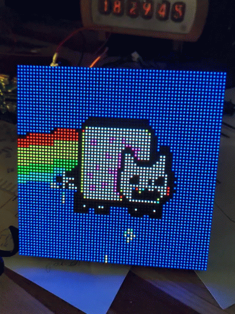
And with that, we should be able to render a nice, smooth animation to our LED panel.

Nyancat in glorious 5-bit colour
As always, full source code to replicate the results of this post is available on Github. If you want more details on the FPGA board used in this post, you can read about it here or take a look at the design files directly here. If you want a refresher on what exactly an FPGA is and does, this post may be useful. If you want to take things to the next level with a soft RISC-V CPU and build your own SoC, click here.